(China (Mainland))

Product Summary
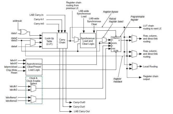
The EP1C12F256C7N contains a two-dimensional row- and column-based architecture to implement custom logic. Column and row interconnects of varying speeds provide signal interconnects between LABs and embedded memory blocks. The logic array consists of LABs, with 10 LEs in each LAB. An LE is a small unit of logic providing efficient implementation of user logic functions. LABs are grouped into rows and columns across the device. Cyclone devices range between 2,910 to 20,060 LEs. The EP1C12F256C7N RAM blocks are true dual-port memory blocks with 4K bits of memory plus parity (4,608 bits). These blocks provide dedicated true dual-port, simple dual-port, or single-port memory up to 36-bits wide at up to 250 MHz. These blocks of EP1C12F256C7N are grouped into columns across the device in between certain LABs. Cyclone devices offer between 60 to 288 Kbits of embedded RAM.
Parametrics
EP1C12F256C7N absolute maximum ratings: (1)Supply voltage With respect to ground, VCCINT: –0.5 to 2.4V; (2)Supply voltage With respect to ground, VCCIO: –0.5 to 4.6V; (3)Supply voltage With respect to ground, VCCA: –0.5 2.4V; (4)DC input voltage, VI: –0.5 to 4.6V; (5)DC output current, per pin, IOUT: –25 to 25mA; (6)Storage temperature No bias, TSTG: –65 to 150℃; (7)Ambient temperature Under bias, TAMB: –65 to 135℃; (8)Junction temperature BGA packages under bias, TJ: 135℃.
Features
EP1C12F256C7N features: (1)2,910 to 20,060 LEs, see Table 1.1; (2)Up to 294,912 RAM bits (36,864 bytes); (3)Supports configuration through low-cost serial configuration device; (4)Support for LVTTL, LVCMOS, SSTL-2, and SSTL-3 I/O standards; (5)Support for 66- and 33-MHz, 64- and 32-bit PCI standard; (6)High-speed (640 Mbps) LVDS I/O support; (7)Low-speed (311 Mbps) LVDS I/O support; (8)311-Mbps RSDS I/O support; (9)Up to two PLLs per device provide clock multiplication and phase; (10)shifting; (11)Up to eight global clock lines with six clock resources available per; (12)logic array block (LAB) row; (13)Support for external memory, including DDR SDRAM (133 MHz),; (14)FCRAM, and single data rate (SDR) SDRAM; (15)Support for multiple intellectual property (IP) cores, including; (16)AlteraR MegaCoreR functions and Altera Megafunctions Partners; (17)Program (AMPPSM) megafunctions.
Diagrams
| Image | Part No | Mfg | Description |  |
Pricing (USD) |
Quantity | ||||||
|---|---|---|---|---|---|---|---|---|---|---|---|---|
 |
 EP1C12F256C7N |
|
IC CYCLONE FPGA 12K LE 256-FBGA |
Data Sheet |
|
|
||||||
| Image | Part No | Mfg | Description | |
Pricing (USD) |
Quantity | ||||||
 |
EP1C12 |
Other |
|
Data Sheet |
Negotiable |
|
||||||
|
EP1C12F256C6 |
|
IC CYCLONE FPGA 12K LE 256-FBGA |
Data Sheet |
|
|
||||||
|
EP1C12F256C6N |
|
IC CYCLONE FPGA 12K LE 256-FBGA |
Data Sheet |
|
|
||||||
|
EP1C12F256C7 |
|
IC CYCLONE FPGA 12K LE 256-FBGA |
Data Sheet |
|
|
||||||
|
EP1C12F256C7N |
|
IC CYCLONE FPGA 12K LE 256-FBGA |
Data Sheet |
|
|
||||||
|
EP1C12F256C8 |
|
IC CYCLONE FPGA 12K LE 256-FBGA |
Data Sheet |
|
|
||||||